
 Microelectromechanical System Essay
Abstract
Microelectromechanical systems (MEMS) are little devices or gatherings of devices that can coordinate both mechanical and electrical segments. MEMS can be developed on one chip that contains one or more microsegments and the electrical hardware for inputs and yields of their parts. The segments incorporate diverse kinds of sensors, transducers, actuators, hardware, and structures. Every kind of segments is intended to interface with the information. For example, it includes light, gas particles, particular kind of radiation, pressure, temperature, or biomolecules. MEMS items became business vicinity. Without a doubt, the pressure sensor and accelerometers in our autos; the ink plane heads in our printers; and the computerized mirror shows in the advanced light projectors (Dlps) are the most prominent and pervasive items to date in our motion picture theaters. With the expanding enthusiasm towards national security, microfluidic frameworks are consistently investigated as an issue to caution unsafe natural operators. In addition to this, they were vigorously investigated in their ability to support synthetic and natural tests. MEMS are being scaled down while less extravagant adaptations of their macro world executive analogs become better. This engineering has developed to the point where the shift from unadulterated exploration to business items can be made.
Microelectromechanical System
1 Introduction
Microelectromechanical systems (MEMS) allude to an accumulation of microseconds and actuators that can sense its surroundings and respond to changes in the environment with the utilization of a microcircuit control. They incorporate, notwithstanding the traditional microelectronics bundling, the coordination of radio wire structures for ordering signals into the microelectromechanical structures for needed sensing and impelling capacities. The framework might likewise require micro power supply, micro hand-off, and micro sign preparing units. Microparts make the framework quicker, more solid, less expensive, and fit for joining more intricate capacities. It is an innovation that can be characterized as scaled-down mechanical and electromechanical components that are made utilizing micromanufacture strategies (Lobontiu and Garcia).
Microelectromechanical frameworks (MEMS) are a procedure innovation used to make minor coordinated devices or frameworks consolidate mechanical and electrical parts. They are manufactured utilizing incorporated circuit (IC) bunch transforming methods and can extend in size from a couple of micrometers to millimeters. These devices or frameworks can sense, control and impel the microscale and create consequences for the macro one. Despite wording, the uniting element of MEMS gadget is standing out in its production process. While the gadget hardware is created the utilization of 'machine chip' IC innovation, the micromechanical parts are manufactured by modern controls of silicon and different substrates utilizing micromachining methods (Maluf and Williams). The exapmles are mass and surface micromachining and also high-viewpoint proportion micromachining (HARM). It specifically evacuates silicon parts or adds extra structural layers to the mechanical and electromechanical segments. While coordinated circuits are intended to use the electrical properties of silicon, MEMS exploits either mechanical ones or both its electrical and mechanical properties.
2 MEM’s Theory and Design
Design is a mix of craftsmanship and science. In the areas where truths and principles are not obviously comprehended or clarified, an outline practice looks like a workmanship that obliges the instinct for perfection. Then again, when a sound learning base in all applicable areas has been entrenched, there is an aphoristic approach that an outline specialist can take after to advance the creation. Because of the multidisciplinary nature and the moderately short history in the relevant developing field, numerous MEMS gadget plan issues are sponsored with a sort of constrained learning base and are usually pretty much an impromptu movement to unavoidable experiencing an experimentation stage. Now and again, the issue explanation is everything except consistent and venture target. It has a constantly moving focus since the disclosures of limits and potential outcomes in MEMS innovations are even now being continually learned.
Due to the profoundly incorporated and interdisciplinary nature of MEMS, it is hard to separate gadget outline from the complexities of manufacture. Subsequently, an abnormal state of assembling and creating information is important to outline a MEMS gadget. Besides, the significant time and costs are used amid this advancement and ensuing model stage. Keeping in mind the end goal of expanding advancement, imagination and diminishing unnecessary 'time-to-market' costs, an overall interface ought to be made to distinguish outline and creation. As fruitful gadget improvement additionally requires demonstrating and reenactment, it is essential that MEMS originators have access to high-quality explanatory devices. Presently, MEMS gadgets use more seasoned configuration apparatuses and are manufactured on an 'experimentation' premise. Thus, all other more effective and progressive instruments' recreation and demonstration are essential for precise expectation of MEMS gadget conduct.
3 MEM’s Materials
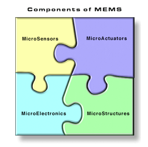
In the most general structure, MEMS comprise of mechanical microstructures, microsensors, microactuators and microelectronics, all coordinated onto the same silicon chip. Initially, MEMS innovation was focused around silicon-utilizing mass micromachining and surface micromachining techniques. Step by step, different materials like, glass, ceramics, and polymers have been adjusted for MEMS (Maluf and Williams). Particularly, polymers are attractive to biomedical applications because of their bio-similarity, simplicity, and suitability for fast prototyping. Other micromachining procedures utilized for creating MEMS incorporate dry plasma drawing, electroplating, laser machining, micro processing, micro embellishment, stereo lithography, and inkjet printing. The materials and systems used as a part of MEMS are persistently advancing.
MEMS engineering is still built generally with respect to acquired procedures from the semiconductor business. A few samples are basically indistinguishable from their semiconductor analogs. Anyway, different methods have been adjusted to satisfy the particular needs. The fundamental issue of a semiconductor process versus a MEMS procedure can be definitely distinctive to the degree that it is habitually impractical or extremely hard to coordinate both hardware and MEMS on the same bit of land. Micromanufactured semiconductor devices are located fundamentally inside the top few microns of the substrate material. MEMS devices may require the whole substrate thickness, the use of its both sides, or even necessitate having different substrates together. Over the years, the range of procedures, that were previously considered to be a piece of the MEMS tool kit, has extended extraordinarily. Customary strategies are still extremely well known yet presently joined by a group of more up to date ones (Lobontiu).
4 MEMs Processing
4.1 Physical vapor deposition (PVD)
PVD covers various deposition advances in which material is discharged from a source and exchanged to the substrate. The two most vital advances are dissipation and sputtering. PVD involves the standard advances of metals. It is much more basic than CVD in terms of metals since it can be performed at lower procedure hazard and be also less expensive concerning materials cost. The nature of the movies is mediocre compared to CVD, which implies higher resistivity of metals and more deserts and traps for protectors. Furthermore, the step scope is not in the same class as CVD. The decision of statement strategy (i.e. dissipation versus sputtering) may often be subjective and depends more on what particular material is capable of at the time in terms of engineering.
4.2 Chemical Vapor Deposition (CVD)
In this process, the substrate is set inside reactor to which various gasses are supplied. The central standard of the procedure is that a concoction response happens between the source gasses. The result of that response is a robust material consolidating on all surfaces inside the reactor. Two most critical CVD advances in MEMS are the Low Pressure CVD (LPCVD) and Plasma Enhanced CVD (PECVD). The LPCVD method produces layers with fantastic consistency of thickness and material qualities (Lee). The principle issues with this method are high working temperature (more than 600°c) and moderate statement rate. The PECVD method can work at lower temperatures (down to 300° C) on account of the additional vitality supplied in the reactor to the gas atoms by plasma. Being realized in such a way, the nature of the movies has a tendency to be subpar compared to the techniques running at higher temperatures. Besides, the most PECVD frameworks can just store the material on one side of a wafer even despite having usually from 1 to 4 waffers. LPCVD frameworks store movies on both sides of minimum 25 wafers at once. A schematic graph of a commonplace LPCVD reactor is demonstrated in the figure below (Lobontiu).
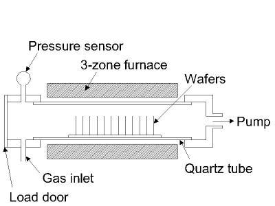
Figure 1: Typical hot-wall LPCVD reactor.
CVD procedures are perfect to utilize when you need a slim film with great step scope. A mixture of the materials can be made with this innovation; nonetheless, some of them are less famous with fabs in light of unsafe repercussions shaped amid transforming. The nature of the material changes from procedure to process; however, important general guideline is that higher temperature yields a material with higher quality and fewer defects.
4.3 Lithography
Lithography in MEMS is regularly the exchange of a photosensitive material by exposing it to radiation source. A photosensitive material is a material that undergoes a change in its physical properties when exposed to radiation. Lithography is a technique by which example exchange can be attained from an expert example of substrate. The central idea has actually been utilized by artisans since late 1700's. Lithography in some structure is commonly the initial phase in many courses of action and, as an issue, is presumably most critical. Photolithography is the most widely recognized innovation, which is utilized, however, as a part of request to stay aware of the determination needs in semiconductor segment. It is insinuated by Moore's Law,with advancing and developing of, for example, X-beam lithography, electron shaft lithography, and particle pillar lithography.
4.4 Photolithography
Photolithography is the process that characterizes and exchanges an example onto a layer of the wafer. In the photolithography transforming a light source is normally used to exchange a picture from a designed cover to a photosensitive layer (photoresist or oppose) on a substrate or flimsy film. The same example is later moved to the substrate or slender film (layer to be carved), utilizing an alternative procedure (engraving method). For a few layers, the opposing example is utilized as an issue for further process. Standard photolithography-based strategies for creating microelectromechanical frameworks display a few disadvantages including cost, incongruence with adaptable substrates, and confinements to wafer gadgets. Microsystems creation utilizes a few layers to construct devices. These layers regularly comprise of slim movies of metal, mass silicon or polysilicon. Photolithography is the procedure stage used to characterize and exchange an example to its particular layer. The photolithographic method happens a few times amid the manufacture of a microsystems gadget as layers expand upon layers. The linkage gathering would require "no less than" six layers. Photolithography is the most widely utilized method as a part of IC industry, for example exchange for multilayered IC's, precise enrollment and uncovering an arrangement of progressive examples.
5 MEMs Applications
Applications of MEMS devices can be found in different businesses, for example, biomedical, aviation, instrumentation, auto, etc. New advancements and applications in the MEMS field are discovering their path into a large number of these businesses consistently. MEMS ended up being a progressive innovation in different fields of the physical area, for example, mechanical (e.g. pressure sensors, accelerometers, and gyroscopes), microfluidics (e.g. inkjet spouts), acoustics (e.g. microphone), RF MEMS (e.g. switches and resonators), and optical MEMS (e.g. micromirrors). Continuously, MEMS engineering has exhibited extraordinary arrangements and also conveyed inventive items in compound natural and medicinal areas, MEMS have entered into buyer's hardware, home apparatuses, car industry, airplane business, biomedical industry, entertainment, and games. Great use of cost proportions is in charge of the fame of mechanical MEMS devices in today's business. They are inalienably faster as velocity typically increases with size. Most MEMS devices work on almost no power so an abnormal state of force utilization is not an issue. These devices additionally reflect large amount of exactness, dependability, and reproducibility. In the assembling MEMS, batch microcreation procedures have influenced the industry and prompted recently in terms of MEMS showcase around the whole world.
5.1 Automotive
In the auto business, MEMS applications hold significant guarantee. Car segments need to be created in expansive volumes from a demands' perspective as well as from the need for recuperating the starting ventures. Working lifetimes of up to 10 years along with low unit costs are additionally needed. These qualities are natural in MEMS devices. Because of the advancement made in cluster assembling of MEMS, huge volumes of profoundly uniform devices can be made taking generally minimal effort. Considered by most designers as bleeding edge or periphery engineering, MEMS sensors have been grasped by the car business in its journey to enhance execution, decrease costs, and upgrade the dependability of a family car. Worth mentioning is also the fact that MEMS sensors have been utilized as parts of autos over the previous decade.
The two key areas where MEMS devices are presently being utilized as parts of autos are in motor control and airbag organization. Complex outright pressure sensors are utilized as a part of motor control in numerous vehicles, and silicon accelerometers are utilized to trigger airbags. Separated from these two MEMS devices being on the vehicles today, there are numerous gadgets that are at different phases of advancement. Some of them will be utilized for the vehicles quite soon. Application areas where MEMS devices may be seen as standard ones include wheel pace sensing, yaw-rate sensing, dynamic security and controlling route, seatbelt prepositioning, street condition observing, etc. A number of these sensors (e.g., MEMS pressure sensors) usually supplant more established advancements with less expensive and more dependable devices. Interestingly, that MEMS inertial sensors have gained numerous attractive gimmicks, which are becoming progressively regular in autos today.
The correct response from air pack control sensor speaks to the biggest car utilization of inertial MEMS sensors. In this application, an accelerometer persistently measures the vehicle's increasing speed. At the point when this parameter goes past a foreordained limit, a microcontroller registers the vital issue of the quickening (i.e., the region under the bend) to figure out whether a substantial net change in speed has happened. The inertial MEMS substance of autos is significant and is developing. As the capacities of these sensors are enhancing, architects are discovering more uses for them to increase the security and unwavering cars' quality. Today, manufacturers principally utilize inertial MEMS sensors to execute the most successful gimmicks (e.g., air sack control), yet execution and accommodation of applications are rapidly turning into a significant business.
5.2 Aerospace
The manufacturing process of airplanes also utilizes MEMS strategies and has two key benefits. Firstly, gadget consistency is high and misfortunes related to mechanical inefficiencies are minimized by the ordinarily high-quality execution of MEMS gadgets (especially if gadget is made with the use of single precious stone silicon as its mechanical material). Besides, MEMS can be utilized to build the actuators' clusters in order to expand the framework advancing. The exhibitions of manufactured planes have been conducted by Glezer and Allens' gatherings at Georgia Tech. They have spearheaded a great part of the engineered plane work including aircraft exhibits created and worked side by side. Microengineering will support lowerpower process and less expensive microinstruments. These economies can help a mixed bag of aviation missions. Batches of MEMS sensors presently incorporate weight, stream rate, speeding up, precise speed, and concoction species determination. For instance, MEMS actuators, valves, manufactured planes, limit layer track gadgets, microplane motors and microthrusters may empower micro Uavs and nanosatellites. The creators have invented and exhibited MEMS manufactured planes and a few microthrusters.
5.3 Biomedical
Another widely known case of the successful MEMS application is the small scale disposable pressure sensor used to screen circulatory strain in healing centers. These sensors interface with a persistent intravenous line and screen the circulatory strain through the IV arrangement. For a small amount of their expenses ($10), they supplant the early outer circulatory strain sensors that cost over $600 and must be cleaned and recalibrated to be used again. These lavish devices measure pulse with a saline-filled tube and diaphragm game plan that must be joined to corridor with a needle. The first MEMS devices to be utilized as a part of the biomedical business were reusable pulse sensors in the 1980s. MEMS pressure sensors have the biggest class of uses including disposable circulatory strain, intraocular pressure (IOP), intracranial pressure (ICP), intrauterine pressure, and angioplasty. A few makers of MEMS pressure sensors for biomedical applications include CardioMEMS, Freescale semiconductors, GE sensing, Measurement Specialties, Omron, Sensimed AG and Silicon Microstructures.
MEMS accelerometers are utilized as a part of defibrillators and pacemakers. A few patients show uncommonly quick or disorganized heart rate. Consequently, they became at a high danger of acute myocardial infarction or a heart assault. An implantable defibrillator restores a typical heart function by giving electrical stuns to the heart under strange conditions. The hearts of some people pulsated too gradually, and this may be identified with the regular maturing procedure or a hereditary condition. A pacemaker keeps up a legitimate heart thumped by transmitting electrical irritants to the heart. Customary pacemakers were altering rate. Thus pacemakers utilize MEMS accelerometers and are equipped with them for altering heart rate as the persistent physical action. Medtronic is a main producer of MEMS based defibrillators and pacemakers. . This pacemaker is intended to be good with attractive reverberation imaging (MRI).
MEMS Hearing-Aid Transducer (a listening device) is an electroacoustic gadget used to open up and emanate sounds into the ear. The objective of this device is to adjust for the impaired hearing and, in this manner, to make sound correspondence more coherent with the client. In the US, listening devices are viewed as medical devices and are directed by the FDA. As for NIH, approximately 17 percent (36 million) of American grown-ups report some level of impaired hearing. There is a solid connection between the patient's age and the reported hearing injury. Additionally, around 2-3 children out of 1,000 are conceived hard of hearing or deaf in the United States. MEMS pressure sensors are likewise consolidated into endoscopes for measuring pressure in the diaphragm and different organs, imbuing pumps for observing blockage, and noninvasive circulatory strain screens. Applications of MEMS pressure sensors inside the biomedical field are various (Maluf and Williams).
5.4 Optical Displays
Digital Light Projector, created and delivered by Texas Instruments, stays one the most creative, mechanically great, and monetary vital MEMS devices fabricated to date. An extensive exhibit of mobile aluminum mirrors is arranged on top of a CMOS memory chip. Cathodes underneath each mirror component permit it to be flipped between two positions because of the substance of the related memory cell. The gadget is the empowering segment in splendid, high determination projection, and it is capable of displaying high definition images.
6 Types of MEMS devices
6.1 Pressure Sensors
A real application for MEMS is mainly sensors. Three essential MEMS sensors are pressure sensors, synthetic sensors, and inertial sensors (accelerometers and gyroscopes). MEMS sensors can be utilized as a part of mixes of different sensors for multisensing tasks. Consequently, MEMS can be composed of sensors to gauge the stream rate of a fluid sample and in the meantime distinguish any defiles inside the specimen. MEMS pressure sensors are intended to quantify outright or differential pressures. They regularly utilize an adaptable diaphragm as the sensing gadget as it may be seen in the picture to the right. One side of the diaphragm is presented to a fixed, reference pressure and the other side is interested in an outside pressure. The diaphragm moves with a change in the outside pressure. MEMS pressure sensors are detailed to work in a mixture of extents, contingent upon the configuration and application. There are MEMS pressure sensors that can gauge pressures close to 0 ATM or 10 ATM or almost 150 psi.
MEMS pressure sensors are sign change, and it enables the utilization of MEMS in different situations. MEMS can also change over physical amounts. For example, wind stream and fluid levels in terms of pressure are measured by an electronic framework. This configuration quality has upgraded the flexibility of MEMS sensors. The normal structure of MEMS fuses a few devices on one chip and permits them to be utilized as a part in various cases. MEMS pressure sensors are utilized in connection with different sensors; for example, temperature sensors and accelerometers for multisensing applications or similar. In reality, a MEMS pressure sensor mounted inside a tire has an uncommon supplying channel of dry air to the sensor's diaphragm.
6.2 Accelerometers (Inertial Sensors)
MEMS inertial sensors can be found in route devices, which are used against shaking. These are high-amplification camcorders, airbag sending frameworks, Apple iPhones, pacemakers, and adjustment frameworks. MEMS inertial sensors are one of the most rapidly developing fragments in the MEMS market. Determined by accelerometer applications like the Apple iPhone and the Nintendo Wii and by the impending enactment obliging solidness control frameworks in all vehicles, these devices have moved out of mechanical portions into customer persuasiveness. MEMS accelerometers use nanotechnology in order to improve the characteristic capacities between all quickening agents; thus, these devices are exact and greatly adjusted.
MEMS accelerometers are really the most straightforward kind since they comprise of minimal seismic mass (otherwise called verification mass) and an additional cantilever shaft. Customarily lingering gas is to be kept inside the gadget, which can result in damping it above the normal conditions. However, it is not very serious unless the Q-component is excessively low. For this situation the damping method can result in a loss of affectability. The instrument works in the following way: outer energy is connected and moves the proof mass from an impartial position to a dynamic position; ordinarily the alteration of this direction is measured by simple or computerized readouts. The varieties can be diagramed by utilizing a set of shafts that are set up diverged from a set of bars being connected to the surface of the evident mass by any means. Such a straightforward framework makes the accelerometer solid as well as generally economical to manufacture.
There have been inquiries regarding the precision of the spring inside the instrument since spring devices can twist or weaken upon weather; it is conceivable to apply an arrangement of piezoresistors to the springs to discover any deformations and guarantee their exactness in this situation. On the off chance, these extra parts are embedded. The assembling procedure is longer and more muddled; thus, gadget becomes marginally pricier. First class MEMS quickening agents are assembled so as to gain the most noteworthy affectability conceivable. These quickening agents are exact enough that they can be measured optically and regardless of their high cost. Consequently, this is perfect research facility gear (International Mechanical Engineering Congress and Exposition and American Society of Mechanical Engineers).
On the other hand, a MEMS quickening agent may be slightly abnormal and have a little warm inside the base of an arch-molded structure which heats the air inside and makes it go up. The vault is furnished with a thermocouple in order to check where the warmed air hits the arch's upper shell. Further, by gauging how far away the air focus is, the level of diversion can be found out. This redirection assessment is a measure of increasing speed, which has been connected to the sensor. Then again, this kind of quickening agent is mostly considered far subpar compared to the previous model. Most accelerometers' capacity is on one hub; however, two-hubs and three-hubs models have been created. The three-pivot model is commonly more extravagant by adding significantly more precision. If this model isn't utilized, three one-hub accelerometers will normally be joined resulting in far less exact metrics. There is additionally an immediate relationship between the quantity of gadgets that can be measured and the precision and affectability of the gadget. Generally, the better the gadget can quantify, the more exact gauges will be displayed.
6.3 Fluid Pumps
Most microfluidic frameworks require an independent dynamic pump of a size practically identical to the volume of liquid to be pumped. The key contemplations they generate are their unwavering quality, power utilization, activation voltage, straightforwardness and the production expenses, biocompatibility, and a dosing exactness equivalent with that of a fuel pump. A common micropump is a MEMS gadget; it is an activation source through which a liquid example (medications and helpful specialists) flows with precision.
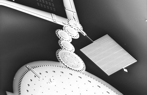
6.4 Gears for Train
The MEMs technology has also been applied to designing of train gears as shown in the figure above.
6.5 Optical Scanners.
Optical MEMS have been effective in terms of display advances. This achievement is quickly developing with the advancements of high definition displays (HD-monitors).
7 Analysis & Conclusion
There are various advantages of MEMS. They incorporate scaling down (permitting appropriated sensing and activation coupled with repetition), decreased production expenses (through the utilization of microelectronics preparing advances), and constant control (permitting on-line dynamic method control and exact checking). Likewise, microdevices can control macroframeworks by utilizing their regular physical enhancement attributes. For instance, the control of stream division at the main edge of delta wings by microactuators permits to control the main edge-vortex position, which determines the lift. MEMS are little devices or their gatherings incorporating both mechanical and electrical segments. It has interminable potential utilizations (Lee). The business sector for MEMS gadgets is even now being created yet does not have such dangerous development as, for instance, the IC business has had in the 1970s.
In spite of MEMS being an empowering engineering for generation and advancing modern items, MEMS is likewise a challenging innovation due to the fact that it differs fundamentally from existing engineering, obliging a totally diverse set of abilities and capabilities to realize it. MEMS includes real scaling, bundling and testing issues; and, as an innovation, confronts difficulties connected with creating assembling procedures that do not fit the existing strategies anymore. For the genuine commercialisation of MEMS, foundries must defeat the discriminating innovative bottlenecks, financial practicality of incorporating MEMS-based parts, and business vulnerability for such gadgets and applications. A toll lessening is also discriminating; it will eventually come about because of better accessibility of its base, more solid assembling procedures, specialized data, and, additionally, new interfacing gauges.

